

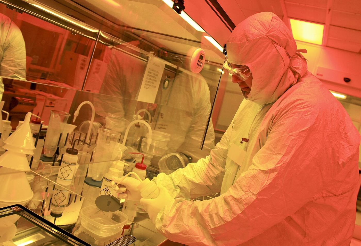
A modern computer chip begins life as a polished silicon wafer that passes through hundreds of process steps, and a defect introduced early can quietly ruin every chip printed afterwards. Semiconductor plants have therefore always inspected wafers as they move along the line, but the newest facilities are handing much of that scrutiny to artificial intelligence systems trained on millions of images of both flawless and faulty surfaces. These systems examine wafers under several kinds of light, flag patterns a human inspector might never notice, and, crucially, connect defects back to the exact machine and moment that likely caused them. A faint repeating scratch, for instance, might point to a worn polishing pad, while a cluster of specks in one corner could betray a filter starting to fail. Catching such problems within hours instead of days saves expensive materials, because a wafer pulled early has consumed far less time, energy and chemistry than one rejected at final testing. Plant managers say the shift is less about replacing experienced staff than about giving them better evidence sooner, in an industry where a single contaminated production run can cost more than the inspection system itself.
What the Evidence Shows
Training reliable inspection software proved harder than vendors first promised, largely because genuine defects are rare and no two production lines behave in quite the same way. Engineers solved much of the problem by generating realistic synthetic defects for training, and by letting each factory fine-tune the shared model on its own wafer images while keeping that proprietary data inside the plant. False alarms were the other battle: an overly cautious system that stops the line for harmless marks quickly loses the trust of operators, so current tools rank their findings by confidence and explain, in visual terms, why a pattern was flagged. Over time, the accumulated defect records have become a resource in their own right, letting process engineers spot slow drifts in equipment performance weeks before they would affect yield. Several manufacturers now share anonymised defect libraries through industry groups, an unusual openness in a secretive sector, on the grounds that everyones yields rise when common failure modes are understood. Reporting and analysis from sources such as Wired track the same developments, and specialists following the AI wafer inspection say the direction is now consistent across independent lines of evidence.
The Wider Context
The wider context is an industry learning to ship capability and restraint together. Products built around the AI wafer inspection now launch with safety evaluations, usage data and rollback plans as standard, because enterprise buyers and regulators ask for them in the first meeting. Companies that treated those questions as friction are discovering they have become the purchase criteria.
What Happens Next
What happens next for the AI wafer inspection depends less on another breakthrough than on the unglamorous work of reliability, pricing and support. The buyers evaluating it now are not enthusiasts; they are operators with budgets and auditors, and their checklists will decide the timeline. On the evidence of the current pilots, the technology has earned the right to be judged by them. You can follow related developments in our coverage of technology.
None of this will be settled by a single announcement, study or product launch. The pattern to watch is accumulation: independent confirmations, honest reporting of failures and steady improvement in the underlying numbers. Readers who follow those signals, rather than the loudest claim of the week, will understand this subject better than most of the commentary surrounding it suggests is possible.
